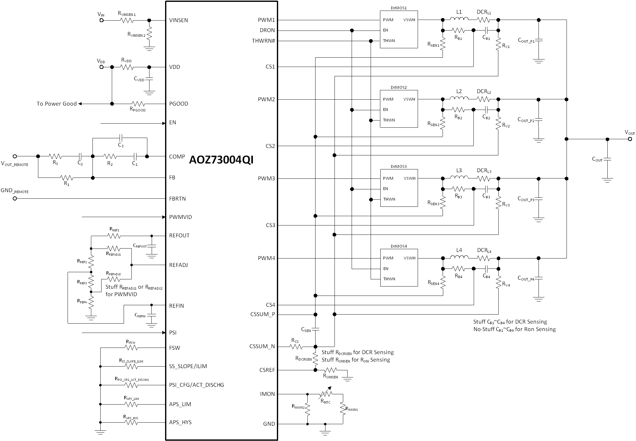
1. System
| Description | Symbol | Value | Unit |
|---|---|---|---|
| Input Voltage | Vin | V | |
| Output Voltage | Vout | V | |
| Switching Frequency | Fsw | kHz | |
| Rated Output Current | Iout_rated | A | |
| Number of DrMOS with PWM1 | PWM1 | ||
| Number of DrMOS with PWM2 | PWM2 | ||
| Number of DrMOS with PWM3 | PWM3 | ||
| Number of DrMOS with PWM4 | PWM4 | ||
| Total Phase | Ph_num |
| Symbol | Value | Unit | SI Value |
|---|---|---|---|
| duty | |||
| ton | ns | ||
| toff | ns | ||
| Tsw | us |
2. Inductor
| Description | Symbol | Value | Unit |
|---|---|---|---|
| Inductor | L | nH | |
| Inductor DCR@25C | DCR | mΩ |
| Symbol | Value | Unit |
|---|---|---|
| DIL | A |
3. Output Capacitor
| Description | Symbol | Value | Unit / Derating |
|---|---|---|---|
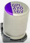 Capacitance |
Cbulk | uF | |
| ESR | ESR | mΩ | |
| # of bulk caps | pcs | ||
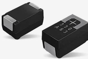 Capacitance |
Cpos1 | uF | |
| ESR | ESR | mΩ | |
| # of bulk caps | pcs | ||
| Capacitance | Cpos2 | uF | |
| ESR | ESR | mΩ | |
| # of bulk caps | pcs | ||
| Ceramic caps (Count & Derating Factor 0–100% ) | |||
| # of 1uF | |||
| # of 2.2uF | |||
| # of 4.7uF | |||
| # of 10uF | |||
| # of 22uF | |||
| # of 47uF | |||
| total output capacitance | uF | ||
| Symbol | Value | Unit |
|---|---|---|
| ripple on C | mV | |
| ripple on ESR | mV | |
| VOUT ripple | mV | |
| Overshoot & Undershoot | ||
| tundershoot | us | |
| Q | uC | |
| tovershoot | us | |
| Q | uC | |
| min. undershoot | mV | |
| min. overshoot | mV | |
| estimated undershoot | mV | |
| GBW | kHz | |
| PM | ° | |
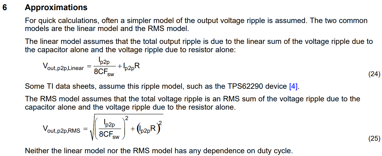
Output Ripple Approximations Reference
4. IMON & Current Sensing
| Description | Symbol | Value | Unit | Note |
|---|---|---|---|---|
| Rated Output Current | Iout_rated | A | ||
| OCP Level | OCL | A | ||
| Current Limit Level set by Pin Strap | ilmt | VIMON @Iout_rated: V | ||
| OCP Margin | ||||
| IMON | ||||
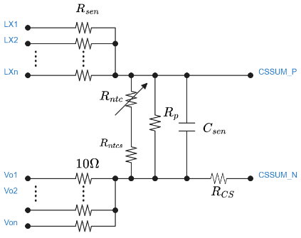
| Min. Current Sense Resistor for CSSUM | RCS_min | Ω | ||
| Current Sense Resistor for CSSUM | RCS | Ω | ||
| Capacitance of CSSUM | Csen | nF | ||
| Ratio of pole/zero | ||||
| Calculated / E96 CSSUM Sense Resistor | Rsen | kΩ | E96: | |
| Choose IMON Temp. Compensation Type | NTC_type | |||
| CSSUM NTC SNR Priority | SNR | |||
| NTC Beta | NTC_β | |||
| NTC Resistance @25°C | RNTC | kΩ | ||
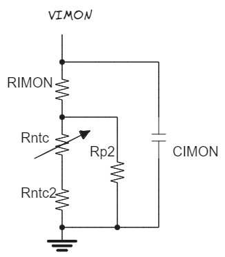
| IMON_NTC_compensation | RC(Rp2) | kΩ | ||
| IMON_NTC_compensation | RS1(Rntc2) | kΩ | ||
| IMON_NTC_compensation | RS(RIMON) | kΩ | ||
| CSSUM_NTC_compensation | RP | kΩ | ||
| CSSUM_NTC_compensation | RNTCS | kΩ | ||
| IMON Resistance setting | max. RIMON,eq | kΩ | ||
| IMON Resistance setting by user selected (close to max. RIMON) | RIMON,eq | kΩ | E96+: kΩ | |
| Capacitance on IMON pin for noise reduction | CIMON | pF | ||
| time constant on IMON pin | τIMON | nsec | ||
| 100%*Iout | A | |||
| Current Limit | A | |||
| Type II NTC compensator | divider ratio | K1 = | ||
CSSUM Circuit & Type II NTC
If CSSUM pin TypeII: changing DCR, RCS, NTC_beta, RNTC, or RIMON updates RP & RNTCS
IMON Pin NTC Compensation (Type II / III)
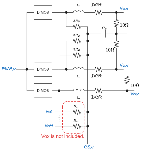
Current Sensing (Per-Phase CSx & Offset Cancellation)
| Description | Symbol | Value | Unit | Info |
|---|---|---|---|---|
| DCR or Ron Sensing | CS_type | RDCRSEN=, RonSEN= | ||
| Offset Cancellation for DCR | DCR_type | node of VOUT: | ||
| Sensing Capacitance for CS | CBx | F | ||
| Sensing Resistance for CS | RBx | kΩ | 1ph: / 2ph: / 3ph: | |
| Additional Resistors for Offset Cancellation | Rm | kΩ |
| Channel | 1 DrMOS / PWM | 2 DrMOS / PWM | 3 DrMOS / PWM |
|---|
1 DrMOS per PWM
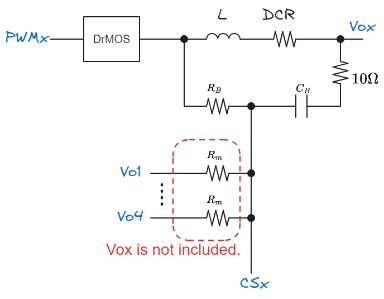
2 DrMOS per PWM
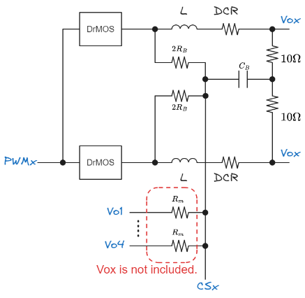
3 DrMOS per PWM
5. APS & PSI_CFG + DCM Check
| Description | Symbol | Value | Unit |
|---|---|---|---|
| PSI Configuration | PSI_CFG | ||
| Set current threshold for 1ph | APS_LIM | A | |
| Set current hysteresis for 1ph | APS_HYS | A |
| DCM Check (Active when PSI_CFG = 0) | Value | Unit |
|---|---|---|
| Ton in DCM | ns | |
| VIMON peak in DCM | V | |
| No double pulses in DCM |
| Threshold | Value | Unit | VIMON |
|---|
6. SoftStart, Active Discharge & Pin Strap
| SoftStart & Active Discharge | Symbol | Value | Unit |
|---|---|---|---|
| Slew rate of soft start | SS_SR | mV/uS | |
| Enable Active Discharge | ACT_DISCHG |
| Pin Strap Resistor | Value | Unit |
|---|---|---|
| R_FSW | Ω | |
| R_SS_ILIM | Ω | |
| R_PSICFG_ACTDIS | Ω | |
| R_APS_LIM | Ω | |
| R_APS_HYS | Ω |
7. Output Voltage Range & PWMVID Circuit
| Description | Symbol | Value | Unit |
|---|---|---|---|
| Min. Output Voltage | Vmin | V | |
| Max. Output Voltage | Vmax | V | |
| Threshold Boot Voltage | Vboot,th | V | |
| Output Voltage when booting (PSI=M) | Vboot | V | |
| Auto-selected PWMVID Type | PWMVID_Type |
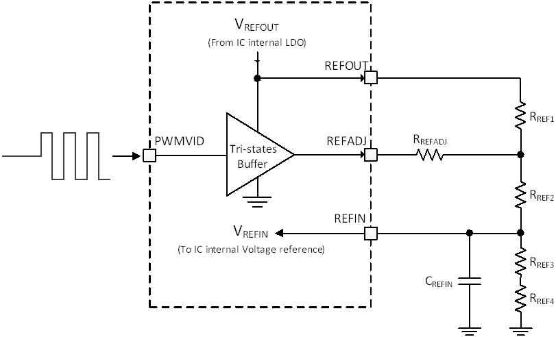
PWMVID Type II (Vboot ≥ Vth)
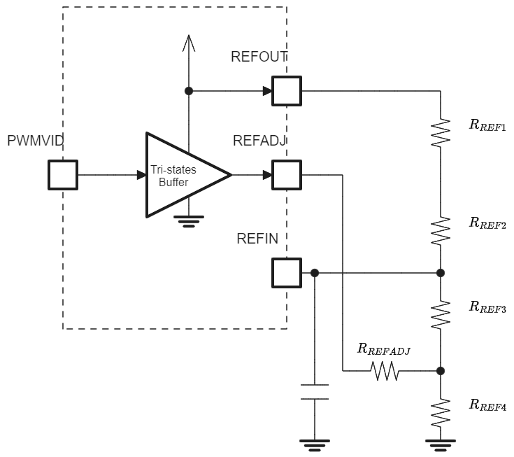
PWMVID Type I (Vboot < Vth)
| PWMVID Type II | |||
|---|---|---|---|
| Top Resistor | R_REF1 | kΩ | |
| Middle Resistor | R_REF2 | kΩ | |
| Bottom Resistors | R_REF3+R_REF4 | kΩ | |
| REFADJ Resistor | R_REFADJ | kΩ | |
| Equivalent R | R_EQ | kΩ | |
| Suggested C_REFIN + C_REFADJ | C_REFIN+ADJ | nF | |
| C_REFIN setting by user selected | C_REFIN+ADJ | nF | |
| max. REFIN ripple @PWMVID=400kHz, 50% | max. VREFIN,pp | mV | |
PWMVID Type II Schematic
| PWMVID Type I | |||
|---|---|---|---|
| Bottom Resistor | R_REF4 | kΩ | |
| Middle Resistor | R_REF3 | kΩ | |
| Top Resistors | R_REF1+R_REF2 | kΩ | |
| REFADJ Resistor | R_REFADJ | kΩ | |
| Equivalent R | R_EQ | kΩ | |
| Suggested C_REFIN + C_REFADJ | C_REFIN+ADJ | nF | |
| C_REFIN setting by user selected | C_REFIN+ADJ | nF | |
| max. REFIN ripple @PWMVID=400kHz, 50% | max. VREFIN,pp | mV | |
PWMVID Type I Schematic
8. Compensator Design & Loop Stability Analysis
| Description | Symbol | Value | Unit |
|---|---|---|---|
| Compensator type | COMP_type | ||
| Gain-bandwidth | GBW | kHz | |
| Phase Margin | PM | ° | |
| Type III available? | |||
| Gain boost | GainB | dB | |
| GainB (V/V) | V/V | ||
| Phase (Plant @ GBW) | ° | ||
| Phase boost | PhB | ° | |
| PhB (rad) | rad | ||
| k factor | k | ||
| pole of compensator | pole | rad | |
| Hz | |||
| zero of compensator | zero | rad | |
| Hz |
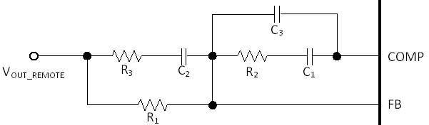
Compensator Schematic
| Method 1: Component Selection (Suggested vs Selected) | |||
|---|---|---|---|
| Item | Suggested | User Selected | Unit |
| R1 | init value | kΩ | |
| C3 | pF | ||
| C1 | pF | ||
| R2 | kΩ | ||
| R3 | kΩ | ||
| C2 | pF | ||
| zero1 (R2, C1) | kHz | ||
| zero2 (R1+R3, C2) | kHz | ||
| pole1 (R3, C2) | kHz | ||
| pole2 (R2, C3//C1) | kHz | ||
| DC gain @ω = 1 rad (dB) | dB | ||
| Method 2: Assign Poles & Zeroes, and DC Gain (Auto-updates Method 1 R/C) | |||
|---|---|---|---|
| Parameter | Input / Value | Unit | Calculated R/C |
| DC gain @ω = 1 rad (dB) | V/V: | edit to sync | |
| zero1 (R2, C1) | kHz | C3 = F | |
| zero2 (R1+R3, C2) | kHz | C1 = F | |
| pole1 (R3, C2) | kHz | R2 = Ω | |
| pole2 (R2, C1//C3) | kHz | R3 = Ω | |
| R1 (Method 2) | kΩ | C2 = F | |
| Loop Stability Metric | Single Phase | Multi-Phase | Unit | w/o VCO (SP) | w/o VCO (MP) | Unit |
|---|---|---|---|---|---|---|
| GBW | kHz | kHz | ||||
| Phase margin (≥45°; w/o VCO >72°) | ° | ° | ||||
| Gain margin (≥6 dB) | dB | PM w/o VCO should be higher than 72° to avoid VOUT ringback | ||||
| Nyquist StbMin (≥0.707) | ||||||
| min Comp. Gain (>8 dB before GBW) | Prevent OVP false trigger when OCL release | |||||
Plant (Gvcvo) Bode Plot
Hover to inspect
plant_gain
plant_gain_SP
plant_Ph
plant_phase_SP
Gc (Compensator) Bode Plot
Hover to inspect
comp_gain
comp_non_gain
comp_Ph
comp_non_ph
min Comp gain (8dB)
○ zero × pole
Loop Gain (Tv) Bode Plot
Hover to inspect
loop_gain
loop_gain_SP
noVCO
loop_Ph
DVS barrier
○ zero × pole
Nyquist Plot (Im{Tv} vs Re{Tv}, -Tv)
Hover to inspect
-Tv(jω)
Unit Circle
× (-1, j0)
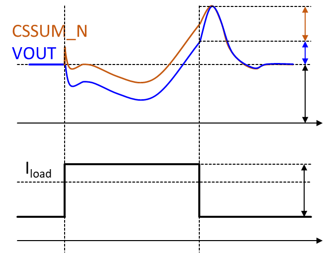
9. Worst Case of OCL-OVP
| Description | Symbol | Value | Unit | Note |
|---|---|---|---|---|
| IC version | ||||
| COMP high clamp during OCL | Vz | V | Internal COMP for OCL is assumed as 2.2V | |
| Voltage offset for OCL release | VOCLR | mV | ||
| Load step to trigger OCL | Istep | A | ||
| Output voltage when OCL test | VOUT,OCL | V | ||
| tovershoot | us | |||
| Q | uC | |||
| Overshoot by load release | VOVS | mV | ||
| Peak of output voltage | VOUT,pk | V | ||
| OVP level | VOVP | V | ||
| OCL-OVP occurs? |
OCL-OVP Waveform
|
10. Internal / Engineering Parameters — Do NOT disclose the below parameters to customers.
| Modulator Parameters | Value | Unit |
|---|---|---|
| Button Enable | ||
| Rramp | ohm | |
| Cramp | F | |
| Rramp * Cramp / Corner | f = Hz | |
| auto gm | ||
| auto gm value | ||
| manual gm | ||
| gm (active) | A/V | |
| Vref | V | |
| Ir | A | |
| If | A | |
| Ir - If | A | |
| Vramp,HB | V | |
| Vramp,LB | V | |
| exp(-ton/RC) | ||
| exp(-toff/2RC) | ||
| Kf | ||
| Kr | ||
| Rsw_on / Rsw_off / Rsw_avg | 1 / 1 |
| Bode Plot & VCO | Value | Unit |
|---|---|---|
| fmin | Hz | |
| fmax | Hz | |
| VCO pole | s | |
| VCO gain | Ω | |
| VCO HPF pole | s | |
| VCO Cg | F |
| Ideal Ramp & EA COMP | Value | Unit |
|---|---|---|
| Vramp,lo | V | |
| Vramp,hi | V | |
| DV | V | |
| COMP Roffset | Ω | |
| internal COMP offset | V | |
| EA COMP | V |
| Measured Duty / Ramp Check (N248:O274) | Value | Unit |
|---|---|---|
| Ron,HS | Ω | |
| Ron,LS | Ω | |
| Vin / Vout | V | |
| Iout | A | |
| ph num | ||
| Iavg per ph | A | |
| D (estimated) | ||
| D (set) | ratio | |
| fsw (meas.) | kHz | |
| ton / toff | s | |
| Vramp,lo (meas) | V | |
| Vramp,hi (meas) | V | |
| DV (meas) | V | |
| EA COMP (meas) | V |